VFD Base Board Assembly Instructions
Follow these instructions to assemble the base board of the VFD Modular Clock.
There are many components to solder, so take your time.
PS: These instructions are for version 1 of the base board. If you find that this does not match your board, switch tothe version 2 instructions
Preparations
Make sure you have sufficient space on your work area. Remove the parts from their packaging. Some of the parts look very similar, so be careful to follow the instructions properly so that the correct part ends up in the correct place.
Some of the components are polarized (such as the electrolytic capacitors), so make sure that you pay attention to polarization when this is mentioned.
We will solder the parts in an order that allows us to test that we are on the right track during the soldering work: Starting with the 5V regulator, then adding the piezo, then the step-up converter that generates the high voltage, and finally the remaining parts.
Step 1: 5V regulator
The clock's main 5V regulated power supply is generated by the TL2575 switching regulator. It provides a nice and stable base power supply for the power hungry VFD tubes.
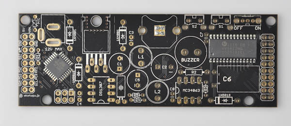
Step 1a:
Let's start with the diode marked 1N4001. It goes in the top left area of the board: If in doubt, the number of the diode is printed on it. The diode has tape on the legs: Remove the tape first, then bend the legs vertically so they fit into the holes in the PCB.
The diodes are polarized and must go in the right way, otherwise the board will not work. The gray band on the diode should match the orientation of the white band printed on the board. The left diode should have the band at the bottom, the right diode should have the band at the top.
Bend the legs and push them through the board. The legs are quite stiff and it can be a bit difficult to get the diode to lie flat against the board. The easiest way to do this is to use pinchers to pull each leg as far as possible, then use your thumbs and push the diode against the board. Bend the legs outward on the back.
Repeat for the other diode. Once both of them are placed, turn the board over to solder all four legs in place. Clip off the excess legs with a flat edge wire clipper.
Be careful when clipping off the legs as they can fly out in unexpected directions: Use eye protection, and hold your hand over when clipping.
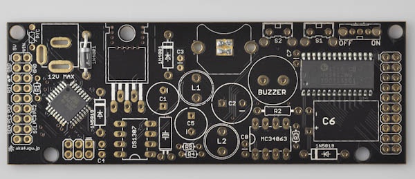
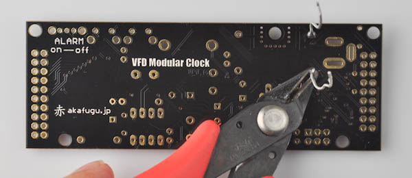

PS: Your kit may include two 1N4001 diodes. If this is the case, discard one of them.
Step 1b:
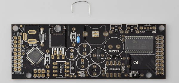
To the right of the rightmost 1N4001 diode, there is a hole marked C3. Take one of the small blue 0.1µF ceramic capacitors (they are marked with the number 104) and place it in this hole, pull it all the way through and spread the legs apart. Now turn the board over, solder the two legs and finally clip off the excess part.
Orientation is not important for ceramic capacitors: It can go in either way.
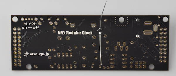
Keep one of the legs you clip off from the capacitor and bend it as shown in the picture above. We will use this in the next step to bridge the footprint that is marked with 1N4001.
Step 1c:
Next, use the leg piece you clipped off from the capacitor in the previous step and place it in the area just left of C3, marked 1N4001.

PS: Earlier kits shipped with two 1N4001 diodes. However, due to the voltage drop of the diode, the voltage level for some boards became too low, causing malfunction in some cases.
See this blog entry for more details
Step 1d:
Now, let's place the voltage regulator, it is the big square part with five legs in a staggered layout. This part is a bit tricky, but be patient and make sure the alignment is proper.
Start by pushing the 5 legs through the PCB, and push them down so that only a few millimeters of the legs stand out. Now, gently bend the regulator backwards. Make sure that the hole on the top part of the regulator matches the hole in the board. (If you prefer, it is also possible to bend the legs before inserting the regulator)
Once the regulator rests snugly against the PCB, attach the screw on the top, and screw in the nut on the bottom.

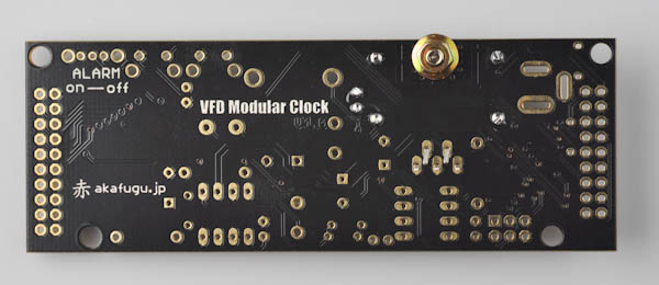
Now, solder the 5 pins and clip off the excess leads. Be careful when clipping off the excess leads here: They are short and are prone to shoot out when you clip them. Use eye protection, and hold your hand over when clipping.
Step 1e:
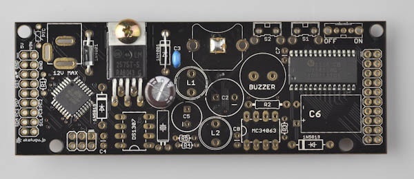
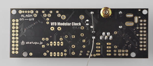
Now locate one of the two brown 47µF electrolytic capacitor. 47µF is printed on the side. It goes into the place marked C1 on the board, to the right of the regulator.
Electrolytic capacitors are polarized and must be inserted the correct way. The long leg of the capacitor goes into the the square hole, and the short leg into the round hole marked with a -.
Push the capacitor all the way through, bend the legs outwards, turn the board over and solder the legs. Finally clip off the excess part.
Step 1f:
Now locate the 330uH inductor. There are two inductors included, so make sure you chose the right one: It has 331 printed on the top.
Orientation does not matter for the inductor: Place it into the place marked L1, to the right of the C1 capacitor you just placed.

The legs of this inductor are short, so the inductor will not stay in place when you turn the board over. The easiest way to hold it in place is to place a small piece of masking tape over it, then turn it around to solder.
First solder one leg, and then check the orientation. If it does not sit flat aginst the PCB, re-apply heat to the leg and nudge it into position. Once you are happy with the orientation, solder the other leg.
You can clip off a little bit from each leg after you solder it if you want: Again be careful of your eyes!
Step 1g:
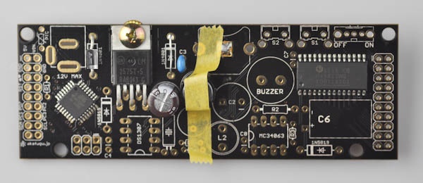
Next is C2. This is for one of the black 330µF electrolytic capacitors. There are two included: Use the smallest one marked 330uF/25V.
The legs are attached a piece of cardboard by tape: Remove this tape first.
Make sure the polarity is correct: The long leg goes into the square hole, the short leg into the round hole with the minus sign. Bend the legs outward to hold in place, then turn over and solder. Finally clip off the legs.

Step 1h:
Now it is time to place one of the two diodes marked 1N5819. It goes on the left part of the PCB between the microcontroller and the regulator.
Make sure orientation is correct: The gray band on the diode must match the white band on the PCB.
Step 1i:
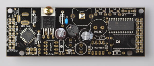
Now let us place the PTC, which is a fuse that protects the board against short circuits and pulling too much current if something goes wrong.
It is a flat yellow disc with the pins placed further apart than the blue 0.1µF capacitors.
NOTE: Make sure not to confuse the PTC with the 1500pF ceramic capacitors. Both have the same color (yellow), but the capacitor is smaller and has the legs closer together than the PTC.
Orientation does not matter for the PTC. When putting the PTC in place you will notice that there is a place where the legs bend inward. Just push the PTC in place until this point, leaving the bend intact. Now bend the legs on the other side of the board outward and solder in place then clip off the excess part of the legs.
Step 1j:
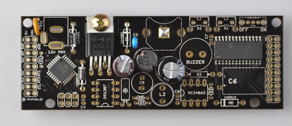
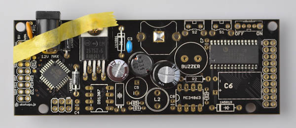
This is the final step to assemble the 5V power supply part of the board. Locate the 2.1mm power plug. It goes in the top left of the board, just right of the PTC. It will not stay in place when you turn the board over on its own: The easiest is to temporarily fasten it with some masking tape.
When soldering it, first put just a little bit of solder on one leg. Check alignment and reapply heat and move the part as needed until the aligment is good. Now solder all three legs fully.
Step 2: Testing the voltage
Insert the plug of the 9V power supply into the socket and turn on power. Wait for a few seconds to make sure everything is ok.
Now, put your multimeter in DC voltage metering mode. On the left-hand side of the board there is a row of 2x9 holes. The two topmost holes are marked 5V and VIN. The next row is marked GND.
Insert the black probe of your multimeter into the GND pin, then the red probe into the 5V hole. Look at the voltage measured: It should be close to 5V. (It will not be exactly 5V since some voltage is dropped against the 1N4001 diode that is attached in series with the output of the regulator). Around 5V is normal, but it may be slightly lower. It must not be less than 4.5V.
Now, move the red probe to the hole marked VIN: It should read around 9V. Depending on the AC adapter, it may be a bit higher or a bit lower, the exact value is not important, but it must be at least 7V for the regulator to function properly.
IMPORTANT: If the voltages measured here are incorrect, do notcontinue to Step 3: Instead go back and double check that all components are inserted correctly and that all solder joints are good.
Once you have checked that the voltage is correct, you may continue on to step 3. Before continuing remove the power jack from the board.
TIP: If you are unable to get the 5V regulator to work, you can always try to post in the forum. There is a dedicated forum for the VFD Modular Clock.
Step 3: Real Time Clock
Before starting step 3, make sure that the clock is not connected to power. It is dangerous to solder the board while power is connected.
Step 3a:
Find the 10kΩ resistor. It is marked with brown, black, orange and gold bars. If in doubt use your multimeter to measure it.
This resistor goes into R1 on the left side of the board, to the bottom left of the power connector. Orientation is not important for resistors. Solder and clip off excess legs as usual.

PS: See here if you are unsure about how to measure the resistance of a resistor.
Step 3b:
Now find the remaining blue 0.1µF ceramic capacitor and place it in the part marked C4 in the bottom left area.
Ceramic capacitors are not polarized so orientation does not matter.

Step 3c:
Next it is time to place the DS1307 real time clock (RTC) chip. There are two 8-pin chips included in the kit, so make sure you select the correct one: It has DS1307 printed on top.
Before placing the DS1307 chip, it may be necessary to bend the legs slightly inward. Hold the chip on its side against a flat surface and press gently. Repeat on the other side.

Now try to insert the chip into the part marked DS1307. The half-circle on the bottom part of the footprint on the board marks the direction the chip needs to be inserted.
The half-circle should match the half-circle indentation in the chip.
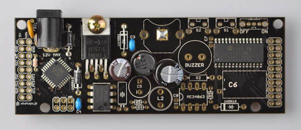
If it is still difficult to insert the chip properly, bend the legs inward or outward to adjust. There will be a gap between the chip and the PCB, but make sure it lies evenly against the board. Now turn it over to solder. If the chip falls out easily, you may use masking tape or clips to hold it in place.
Once again, solder one leg first, then adjust alignment if neccesary. Once alignment is good, solder the remaining legs.
Step 3d:
Now find the 32kHz crystal: It is a small shiny cylinder. Bend the legs so that they stand 90 degrees against the part, then insert it into the footprint to the right of the DS1307 chip. The crystal is not polarized so it can go in any way.

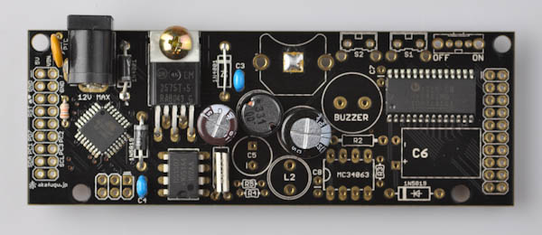
Don't worry if the crystal ends up pointing upward slightly.
Step 3e:
Now find the piezo: It is the large black disk with a hole in the middle. Remove the tape from the piece of cardboard attached.
It goes into the part marked BUZZER on the board, in the top right area. Orientation is not important. Bend the legs outward to hold it in place while soldering.
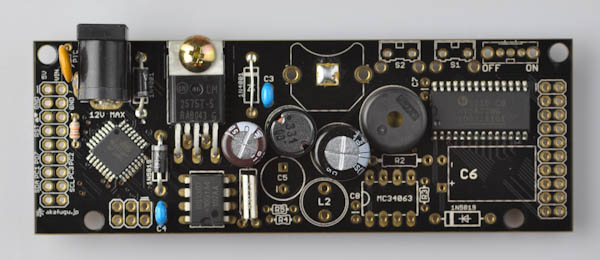
Step 3f:
Locate the place for the battery holder in the top middle of the PCB. You will notice that there is a bit of solder on the center pad already. Leave that in place, as it will help get better contact with the battery.
Now place the battery holder: Orient it as shown in the outline on the board. To prevent it from falling out while soldering place clips or some masking tape over it.
Solder only one leg first, and check orientation. If you are not happy, re-apply heat and adjust. Be very careful: Since the entire area of the battery holder is metal it conducts heat very quickly, so allow it to cool down before touching it.
Once both legs are soldered properly, wait a little bit again for it to cool down.

Now it is time to place the battery. The part of the battery marked + should face upward (there is a + printed on the battery holder to remind you of this). Slide it all the way in. The battery will keep the real time clock running even when the clock has no power.
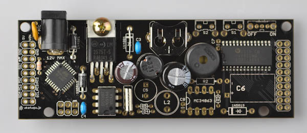
Push the battery all the way in.

Step 4: Checking that the microcontroller operates
Apply power once again. Now you should hear three beeps as the microcontroller boots. If not, go back and double check that all the parts have been inserted properly and that all the solder joints are good.
Do not proceed to step 5 until you are able to hear the beep.
Remove power before continuing! (You may leave the battery in place)
Step 5: Boost Converter
Next it is time to build the boost converter. The boost converter takes the 9V from the AC adapter and converts it to the 25 volts required to light up the VFD tubes.
Step 5a:
Find the remaining 47µF electrolytic capacitor (brown) and place it in C5: Long leg goes in the square hole, short leg in the round hole.

Step 5b:
Find the remaining 2.2mH inductor. It has 222 printed on the top.
It goes into L2. It is not polarized and can go either way.

Step 5c:
Find the 1500pF ceramic capacitor: It has a yellow head to distinguish it from the other ceramic capacitors. It goes into C8, just right of the 2.2mH inductor.

Step 5d:
Now place the boost converter chip in the part marked MC34063 (or 063EC, depending on manufacturer). This chip doesn't have a half-circle indentation like the DS1307: Instead it just has a small dot on one side: The dot should be on the same side as the half-circle on the PCB (pointing left).
Like with the DS1307 chip, it will probably be neccesary to bend the legs inward slightly before inserting the chip.
Step 5e:
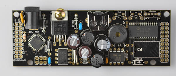
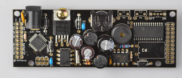
Now let us place all the remaining resistors. Be very careful that all the resistors go into the right place, otherwise the output voltage of the boost converter will not be correct! Some of the colors printed on the resistors can be a bit hard to make out, so If in doubt, use your multimeter to measure each one!
- The 47kΩ (Yellow, Violet, Orange, Gold) resistor goes into R5.
- The 1.6kΩ (Brown, Blue, Red, Gold) resistor goes into R4.
- The 180Ω (Brown, Gray, Brown, Gold) resistor goes into R3.
- The 0.22Ω (red, red, gray) resistor goes into R2. (this resistor is bigger than the others).
PS: Older kits were shipped with a 2.4kΩ (Red, Yellow, Red, Gold) instead of the 1.6k resistor.

Place all the resistors, bend the legs, solder and clip off the excess parts.
Step 5f:
Find the final 1N5819 diode: Place it so that the gray bar faces to the left, maching the white bar on the PCB. It goes in the lower right of the PCB.
Step 5g:
Find the big 330µF / 50V electrolytic capacitor and remove the piece of cardboard it is taped to.
It will be placed lying on its side: Bend the legs 90 degrees.
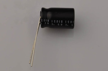
Now insert it into the big part marked C6. Make sure the long leg goes into the square pin marked + and the short leg into the round pin marked - (in other words, the 90 degree bend must be in the correct direction!)

Step 6: Testing the boost converter
Insert the 9V power supply once more. Again you should hear three beeps.
Set your multimeter to DC voltage mode and place the black ground probe in one of the pins on the left side marked GND.
Again, double check the 5V and VIN voltages: They should be about the same as before.
Now, place the red probe so that it touches on the left side of the 1N5819 diode in the bottom right part of the board. The voltage should read about 38 volts.
Now, keep the red probe in contact with the diode and remove power (or, if this is difficult, turn off power, and then touch the left side of the diode again.
You should be able to see the voltage dropping gradually. Once the voltage is down to a couple of volts, you can continue to the next step.
PS: If your kit shipped with a 2.4k resistor instead of a 1.6k resistor, the high voltage will read around 26 volts.
Step 7: Finishing touches
Make sure power is removed before continuing!
Step 7a:
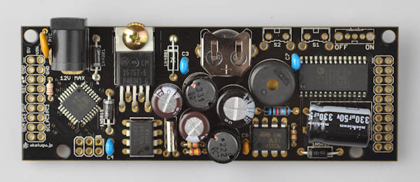
Place the final 0.1µF ceramic capacitor in C7, in the top right area.
Step 7b:
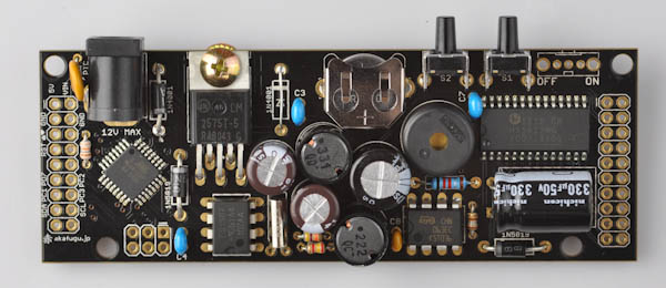
Place the two buttons S1 and S2, the button part should point upward. Push them all the way in so that they stay in place while soldering.
Step 7c:
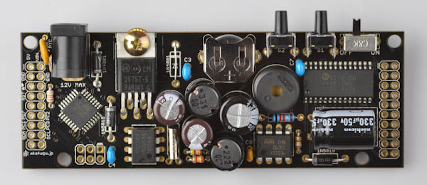
Place the slide switch in the top right, nob pointing upward. Use clips or some masking tape to hold it in place while soldering.
Slide the switch to the left after soldering it.
Step 7d:
Now only the two female headers remain. Place them so that they point upward: The 2x9 one goes on the left side, the 2x10 one on the right side. They are symmetrical, so direction doesn't matter.
Use clips or masking tape to hold them in place while soldering. As always, solder one leg first and adjust alignment if neccesary.

CONGRATULATIONS: You have assembled the VFD Modular Clock Base Board.